

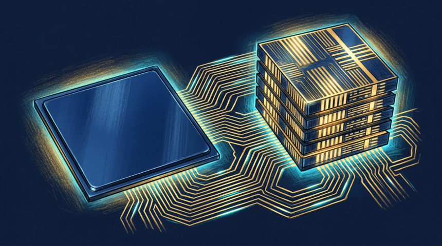
Amazon’s chip arm is the first customer for a NVIDIA memory design that rearranges where the controller lives. NVHBM, built under NVIDIA’s NVLink Fusion program, moves the memory controller off the compute die and embeds it in the base die of the 3D HBM stack.
The payoff is threefold, per NVIDIA: memory bandwidth up 30 percent, HBM power draw down 15 percent, and up to 25 percent more room on the XPU die for compute, all compared with standard HBM4E. Controller logic no longer eats silicon that could be doing math.
Multiple memory vendors will offer the same standardized NVHBM implementation, which NVIDIA says trims integration and qualification work for custom chip builders. The first adopter is Annapurna Labs, whose Trainium4 accelerators will join the NVLink Fusion ecosystem with NVHBM on board, putting AWS hardware and NVIDIA GPUs in the same rack architecture.
The move signals that hyperscalers increasingly want semi-custom systems, mixing their own accelerators with NVIDIA’s platform inside shared racks.